 Menu
Menu


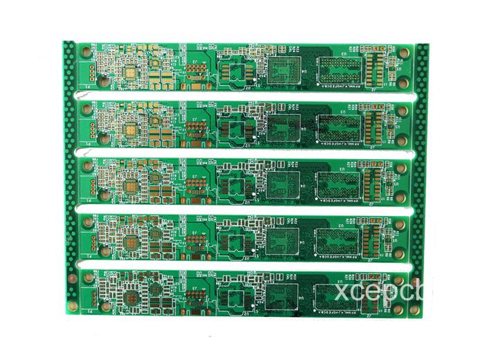
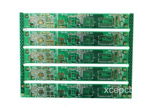

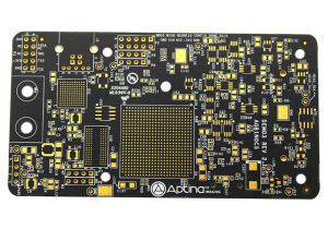
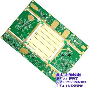
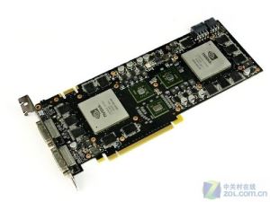
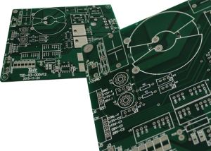
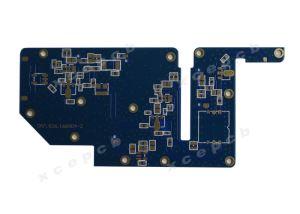
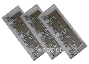
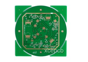
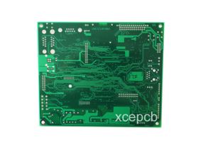
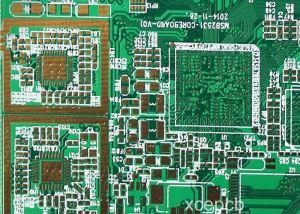
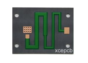
16 Multilayer Metal Hole PCB Board With 8mil Min Line Width In Green Soldermask
-
Min Order
1
-
Product Unit
Pieces
-
Origin
China Mainland
-
Payment


- Contact Now Start Order
- Favorites Share
- Description
Product Detail
16 multilayer metal hole PCB board with 8mil min line width in green soldermask
pp sheet is a prepreg (Prepreg is Pre-pregnant abbreviation), is a synthetic resin with the carrier sheet adhesive material. A. resin - is a thermosetting material for polymers, currently used as an epoxy resin. It has three life cycle to meet the requirements of the platen: A-Stage: brominated Bisphenol + epichlorohydrin liquid epoxy resin for the A-Stage, also known as varnish (Varnish). B-Stage: with glass fiber sizes in A-stage resin, after hot air or infrared drying, partial polymerization, into a solid film, called B-Stage.
BGA stands for Ball Grid Array (PCB ball grid array structure), it is a large, pin package assembly, four pin QFP and similar, are using SMT solder paste to the circuit board is connected. Their differences are listed in the surrounding "space was the" single-row pin, such as gull wing room to move, room to move flat or retracted abdomen and foot end of the J-; changed to the bottom belly full array or an array of local, the adoption of a two dimensional area of the solder ball pinout, as the chip package on the circuit board solder interconnection tools. It has an area of less packaging, increased functionality, increased pin count, high reliability, good electrical properties, low overall cost.
The outer line of the BGA production:
BGA can refer to specifications, design pad size corresponding to the position of a customer to make a standard design BGA BGA array, and then as its benchmarks to be corrected under the BGA and BGA vias were being shot, to be filmed after the original is not shoot before the backup check the level of contrast before and after being shot effect, if BGA pad around large deviations, can not only beat BGA position over the next hole.
Model Number:XCEPCB0016
Shipping port:ShenZhen/HongKong
Place of origin:GuangDong,China
Delivery Time:3-10 Working Days
Production capacity:FR4:2000000Sqms High Frequency board:10000Sqms
Price Terms:FOB
Minimum Order Quantity:1pc
Payment terms:TT,Paypal,Western Union
Certification:CE,ROHS,FCC,ISO9008,SGS,UL
Material:FR4 | Soldermask:Green |
Molde Number:xcepcb0016 | Silkscreen:White |
Layer:16 | Panel Size:300*205mm/5pcs |
Board Thickness:1.6mm | Package Details: Inner:Vacuum-packed Bubble bag With Foam Outer:Carton Box |
Min Line Space:8Mil | |
Min Line Width:8Mil | |
Min Hole Size:18Mil | |
Finished Surface:ENIG | Special requirement: BGA Prepreg Provide Slice report |
Finished Copper:1oz | |
Delivery Time:8 Days |

Shenzhen Xinchenger Electronics was a leading manufacturer of high frequency and high difficult pcb circuit board for many years in shenzhen.We have newest pcb machine like laser drill machine,can do min2mil line space and width for you.
With these top technology,we can meet all your requirements,such as 24 hours quick sample service,rogers&fr4 mixed compression,4-28 multilayer lamination,crossed blind buried vias hole and so on.
Any inquiry can feel free to send us to check if we are able to manufacture your boards.We have professional engineer with more than 10 years pcb working experience can understand all your detail requirements whatever Chinese or English.
Via Hole ", ie, vias, refers to a multilayer circuit board only as a hole between the layers conductive interconnect applications, generally no longer used for welding parts of the foot insert Such holes through the" Shen copper "step in the hole plated with a layer of copper for conductivity.
These vias penetrating the entire board "all through vias" (Through Via Hole), have turned to the board only without all through "blind vias" (Blind Via Hole), there is no contact with the plate surface Tong was buried in the inside of the plate, "buried through holes" (buried Via hole) and the like. These complex partial vias is sequentially continuous legal pressure (Sequential Lamination) produced complete. This term is also often referred to as "Via".
The main parameters of the substrate (Copper-Clad Laminate copper clad substrate) (in KB-6160 (the most commonly used FR-4 plate), for example)
Yellow and white core plate divided core material, usually white core material;
Sheet Size: 36 "* 48", 40 "* 48", 42 "* 48", 37 "* 49", 41 "* 49", 43 "* 49";
Thickness: 0.10mm, 0.10MM behind by increments, usually the thickest of 3.20mm, 0.30mm or less can do multilayer core board, 0.60MM surface treatment can not do the following HAL, complete the following press thickness 1.00mm thickness the thickness of ± 0.10,1.00mm by more than ± 10%;
Sheet copper thickness: 1 / 3OZ-12um, 1 / 2OZ-17.5um, 1OZ-35um, 2OZ-70um, 3OZ-105um, etc;
TG value: glass transition temperature, the material begins to be interpreted as a softening point of the glass as the temperature in the molten state. Normal TG (=140 ?), the TG (150 ?), high TG (=170 ?)
CTI Definition: comparative tracking index; divided into six grades: 1 (CTI=600V), 2 (600V> CTI=400V), 3 (400V> CTI=250V), 4 (249V> CTI=175V), 5 ( 175V> CTI=100V), 6 (100V> CTI=0V);
Dielectric constant (Er): general value 4.2-4.5;
Thermal decomposition temperature (TD): typ. 305 ?;
Parameter:
Layer No. | 1-16 |
Min board thickness | 2 layer 0.2mm |
4 layer 0.4mm | |
6 layer 0.6mm | |
8 layer 0.8mm | |
10 layer 1.0mm | |
Max panel size | 508*610mm |
Board thickness tolerance | T=0.8mm±8%,T<0.8mm±5% |
Wall hole copper thickness | >0.025mm(1mil) |
Finished hole | 0.2mm-6.3mm |
Min line width | 4mil/4mil(0.1/0.1mm) |
Min bonding pad space | 0.1mm(4mil) |
PTH aperture tolerance | ±0.075mm(3mil) |
NPTH aperture tolerance | ±0.05mm(2mil) |
Hole site deviation | ±0.05mm(2mil) |
Profile tolerance | ±0.10mm(4mil) |
Board bend&warp | =0.7% |
Insulation resistance | >1012Onormal |
Through-hole resistance | <300Onormal |
Electric strength | >1.3kv/mm |
Current breakdown | 10A |
Peel strength | 1.4N/mm |
Soldmask regidity | >6H |
Thermal stress | 288?20Sec |
Testing voltage | 50-300v |
Min buried blind via | 0.2mm(8mil) |
Outer cooper thickness | 1oz-5oz |
Inner cooper thickness | 1/2 oz-4oz |
Aspect ratio | 8:1 |
SMT min green oil width | 0.08mm |
Min green oil open window | 0.05mm |
Insulation layer thickness | 0.075mm-5mm |
Aperture | 0.2mm-0.6mm |
Competitive Advantage:
1) With UL,ROHS,ISO,IPC
2).Lead time:3-10 working days
3)Competitive price best quality
4).Rich 20 years experience in High Tg Multilayer PCB .
What Information customer need to provide for quotation ?
1. PCB Gerber files ,protel,powerpcb,Autocad,etc.
2. BOM list for PCB assembly.
3. Send us your sample PCB or PCBA.
4. OEM is acceptable.
Contact Information:
Karen-Sales Department
ShenZhen Xinchenger Electronics Co.,Ltd
sales3@xcepcb.com
Skype:karen-xcepcb
Website:www.fr4-pcb.com/www.xce-pcb.com
Xinchenger Electronics is a professional manufacturer of high-tech products who can offer you 16 multilayer metal hole pcb board with 8mil min line width in green soldermask with competitive price. Just be free to buy good 16 multilayer metal hole pcb board with 8mil min line width in green soldermask at reasonable price with us and get the datasheet from our suppliers who can working for you.
-
Shot Blasting Machine For Engineering Machinery And Automobile Industries 1 Pieces / (Min. Order)
-
Automatic Flatbed Die Cutting Machine For Self Adhesive Labels 1 Pieces / (Min. Order)
-
Automatically Garment Screen Printing Machine For Garments 1 Pieces / (Min. Order)
-
CNC Cutting Machine-roller Horizontal Splitting Machine R Series 1 Pieces / (Min. Order)
-
Automatic Wire Cutting Angle Window Patching Machine WH-1000BS 1 Pieces / (Min. Order)
-
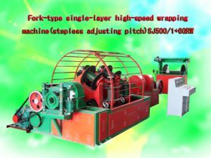
Fork-type Single-layer High-speed Wrapping Machine(stepless Adjusting Pitch)SJ500 1+6GRW 1 Pieces / (Min. Order)
-
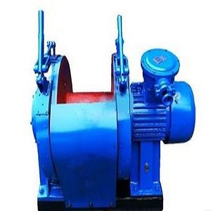
T12-points Mooring Positioning Winch For Offshore Platform 1 Pieces / (Min. Order)
-
LT-S1 Manual Simple Pen Curve Screen Printing Machine For Round Products 1 Pieces / (Min. Order)
-
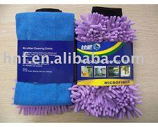
Drying washable microfiber cleaning cloth mop for cars 1 Pieces / (Min. Order)
-
Special Liquid Silicone Injection Molding Machine120 Tons 1 Pieces / (Min. Order)
-
Second-hand Injection Molding Machine 350 Tons 1 Pieces / (Min. Order)
-
Second-hand Injection Molding Machine Fanuc S2000i 250B 1 Pieces / (Min. Order)
-
Building Materials White Ink Inkjet Printer 1 Pieces / (Min. Order)
-
Slitting Machine Slitter Machine Leveler Machine Kaiping 1 Pieces / (Min. Order)
-
PRW Tipping Paper With Unit Type Rotogravure Press 1 Pieces / (Min. Order)
-
YLL /YGL Liquid Phase Chain Grate Vertical Coal-fired Heat Transfer Fliud Furnace 1 Pieces / (Min. Order)

-
YLL/YGL Liquid Phase Chain Grate Vertical Biomass-fired Heat Transfer Fluid Furnace 1 Pieces / (Min. Order)
-
Full-automatic Centrifugal Casting Machine With Three Mouuld-heads 1 Pieces / (Min. Order)
-
630B Semi-autommatic Centrifugal Casting Machine With Theree Mould-heads 1 Pieces / (Min. Order)
-
MX-618B Semi-automatic Centrifugal Casting Machine With Single Mould-head 1 Pieces / (Min. Order)
 Favorites
-
 Tg170, Lead Free Telecom 4layer PCB
1 Pieces / (Min. Order)
Tg170, Lead Free Telecom 4layer PCB
1 Pieces / (Min. Order)
-
 FR4 PCB 1.6MM Thickness Lamps And Lanterns Application
1 Pieces / (Min. Order)
FR4 PCB 1.6MM Thickness Lamps And Lanterns Application
1 Pieces / (Min. Order)
-
 High power amplifier Taconic board
1 Pieces / (Min. Order)
High power amplifier Taconic board
1 Pieces / (Min. Order)
-
 High Power Amplifier Taconic Board 0.508mm
1 Pieces / (Min. Order)
High Power Amplifier Taconic Board 0.508mm
1 Pieces / (Min. Order)
-
 rogers5880 high frequency pcb board
1 Pieces / (Min. Order)
rogers5880 high frequency pcb board
1 Pieces / (Min. Order)
-
 Rogers PCB 8 Layer Prototype PCB
1 Pieces / (Min. Order)
Rogers PCB 8 Layer Prototype PCB
1 Pieces / (Min. Order)
-
 PCB assembly OEM service for home appliances
1 Pieces / (Min. Order)
PCB assembly OEM service for home appliances
1 Pieces / (Min. Order)
-
 PCB assembly for LED products
1 Pieces / (Min. Order)
PCB assembly for LED products
1 Pieces / (Min. Order)
-
 6 Layers-Automobile PCB
1 Pieces / (Min. Order)
6 Layers-Automobile PCB
1 Pieces / (Min. Order)
-
 High Quality PCB for Electronics Projects
1 Pieces / (Min. Order)
High Quality PCB for Electronics Projects
1 Pieces / (Min. Order)
-
 PCB for High Frequency Devices
1 Pieces / (Min. Order)
PCB for High Frequency Devices
1 Pieces / (Min. Order)
-
 Rogers 6006 High Frequency PCB Prototype
1 Pieces / (Min. Order)
Rogers 6006 High Frequency PCB Prototype
1 Pieces / (Min. Order)
-
 Rogers 3010 And 3035 Series
1 Pieces / (Min. Order)
Rogers 3010 And 3035 Series
1 Pieces / (Min. Order)
-
 BGA 14 Layer Electronic Board For Electronic Products In Green Soldermask
1 Pieces / (Min. Order)
BGA 14 Layer Electronic Board For Electronic Products In Green Soldermask
1 Pieces / (Min. Order)
-
 HDI High TG 24 Multilayer Immerison Gold Inner 0.5oz Outer 1oz PCB Board
1 Pieces / (Min. Order)
HDI High TG 24 Multilayer Immerison Gold Inner 0.5oz Outer 1oz PCB Board
1 Pieces / (Min. Order)
-
 Carbon Oil PCB Board With Counter Sunk Hole For 10 Multilayer PCB Board
1 Pieces / (Min. Order)
Carbon Oil PCB Board With Counter Sunk Hole For 10 Multilayer PCB Board
1 Pieces / (Min. Order)
-
 Blind Hole With Blue Soldermask TG140 Printed Circuit Board 10 Layer Circuit
1 Pieces / (Min. Order)
Blind Hole With Blue Soldermask TG140 Printed Circuit Board 10 Layer Circuit
1 Pieces / (Min. Order)
-
 Blind Vias PCB
1 Pieces / (Min. Order)
Blind Vias PCB
1 Pieces / (Min. Order)
-
 RT Duroid 5880
1 Pieces / (Min. Order)
RT Duroid 5880
1 Pieces / (Min. Order)
 Frequent updates ensuring high quality data
 Over 5000 customers trust us to help grow their business!


 Menu
Menu